2018-08-30
2018-09-01
One of the current and hopefully last hardware niggles is the unexpected value on the last analog input. It’s consistently reading millivolts higher than the other analog inputs. This has been verified with and without a device attached to it.
The analog input in question is ICD4. Because I took a thing naming class at a community college, you can be absolutely clear that this is the fourth ICD input. When nothing is connected to this input, the input is (or should anyways) be pulled down to zero (ground).
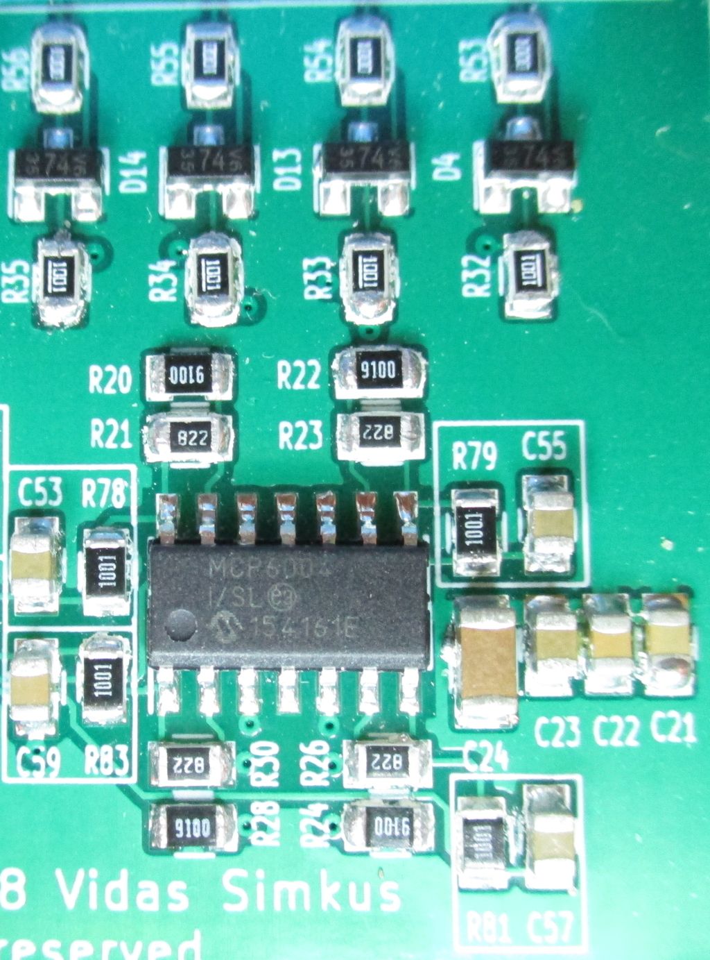
Here is the whole circuit in question. Yet again, sorry for the potato cam, but I gotta say that these shots turned out not too bad (for a potato).
Going from the top down; at the very top is the terminal strip.
Resistors R53-R56 (very top) are the current limiting resistors for the over/under voltage clamping diodes immediately bellow them. Resistors R32-R35 are the 1K load resistors that the ICD probes terminate at. R20-R23 are part of the feedback network. C53/R78 and R79/C55 are the low pass filters for two of the opamp outputs. The black IC int he middle is the actual opamp – Microchip MCP6004. C59/R83 is another low pass filter. R24,26,28,30 are the feedback network resistors for two more feedback networks. C21-C24 are bulk and decoupling caps. Finally R81/C57 is the last low pass filter.
Before you start hating on the solder quality, these were all done by hand. So keep it to your self.
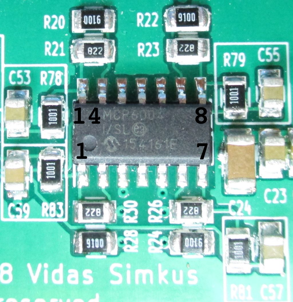
In case you have forgotten the pin order on a 14 pin package, here’s a reminder:
I went through and measured all of the pin voltages. Here’s the table with all of the pertinent information.
| Pin # | Name | Map | Value |
| 1 | VOUTA | uC ICD1 AI | 0.0049 |
| 2 | VINA- | ICD1 Feedback | 0.0005 |
| 3 | VINA+ | ICD1 input | 0 |
| 4 | VDD | 5V | 4.993 |
| 5 | VINB+ | ICD2 input | 0 |
| 6 | VINB- | ICD2 Feedback | 0.0006 |
| 7 | VOUTB | uC ICD2 AI | 0.0059 |
| 8 | VOUTC | uC ICD3 AI | 0.0054 |
| 9 | VINC- | ICD3 Feedback | 0.0005 |
| 10 | VINC+ | ICD3 input | 0 |
| 11 | VSS | GROUND | 0 |
| 12 | VIND+ | ICD4 input | 0 |
| 13 | VIND- | ICD4 Feedback | 0.0011 |
| 14 | VOUTD | uC ICD4 AI | 0.0112 |

From: http://www.ti.com/lit/an/sloa059/sloa059.pdf
Input Offset Voltage Defined
The input offset voltage is defined as the voltage that must be applied between the two input
terminals of the op amp to obtain zero volts at the output. Ideally the output of the op amp should
be at zero volts when the inputs are grounded. In reality the input terminals are at slightly
different dc potentials.
…
VIO is always multiplied by the noninverting gain of the op amp and added to (or subtracted from)
the signal gain of the circuit, which is –(RF /RG) in this example.
2018-09-01: We interrupt this regularly scheduled broadcast to bring you this news.
This is a much better explanation here <very long and convoluted URL> [link is broken as of 2021-11-11]
Quote:
In an operational amplifier, the input offset voltage is the difference in the voltage between the + and – input pins when negative feedback is applied. In a comparator, the input offset voltage is the comparison voltage (threshold voltage) error.
Although ideally 0, in an operational amplifier, there is a difference between VBE of the + and – input transistors in the input-stage differential amplifier, which becomes the input offset voltage.
In actual use; for example when using an operational amplifier with an input offset voltage of VlO ≤ ±5mV, if ×100 amplification is created, there will be an error of up to ±5×100= ±500mV at the output. Therefore, when using a circuit that handles very small input signals, you must either select a product with a small input offset voltage, or adjust the offset externally.
Well shit. Look like I’m chasing my tail around. Hurray for learning!
The way I’m interpreting the situation, the input offset voltage is simply the property of my opamp that I chose based on price (the more lower the more better!) and manufacturer.
In all fairness though the opamp is perfectly fine for what I’m using it for. This sort of thing is exactly why I built in software-based calibration into the design.
Next step is to figure out why my ADC readings are off by a few millivolts.