2017-09-30
2017-09-30
How do I put this. Version 1 of the board is done. The pictures below is the first board assembled on the final revision of the PCB. It says revision C, but it’s really revision D. The only difference between C and D is that I made the holes slightly bigger for the drive FETs in the output over-current protection circuits.
This batch I had manufactured by Elecrow (https://www.elecrow.com/). I’m fairly satisfied with the results. The main issue is the silkscreen quality. On the OSHPark boards it’s laser-sharp. On these it’s mostly readable, but the smaller print is a bit funky. Another issue is that some of the annular rings are a bit off center. Overall, the board is fully functional and the 1/3rd of the price makes up for a lot of imperfections. The OSHPark boards cost me $30.63 per board while the Elecrow boards coast me $8.33 per board, with all shipping included. If I decide to do another batch I will make the smallest silkscreen print a bit bigger and perhaps investigate Electrow’s “premium” PCB service. One of the bullet-points in their premium service description is higher quality silkscreen.
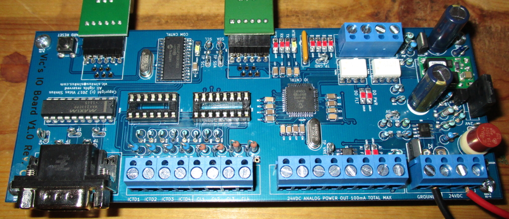
The artistic 11/16th view. This is during the initial programming of the board. The ADC input low-pass-filter resistor network and the op-amp have not been jammed in their sockets yet.
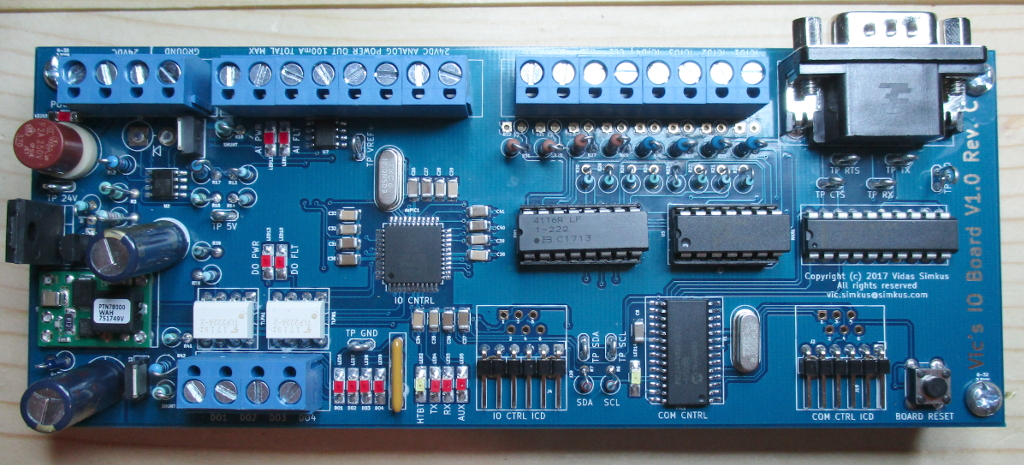
Completely programmed and populated board. I really like the blue solder mask. The lighter color makes the traces stand out more.
Backside of the board. I really really like the visibility of the traces.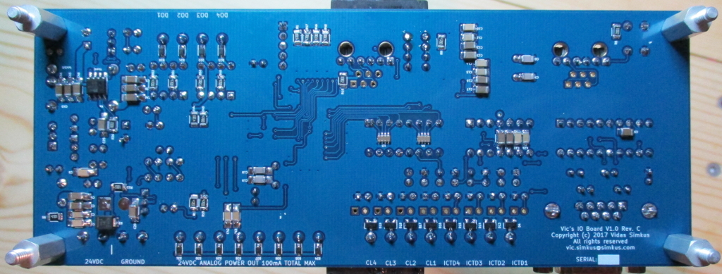
The next step is to assemble two more complete boards and partially populate the remaining PCBs with the surface mount components. That will give me four complete boards – one dev board, two production, and one spare in case I blow the ass out of one of the other three. The partially completed boards will eliminate the most time consuming step of assembly in case I need to spin up a board in the future.
Software-wise I want to implement two levels of calibration with the data stored on the board it self. The first level would be to account for the variations of the board hardware. The second level would account for the variations in the sensor. So what I’m thinking is level one calibration would be done with 1V being put on the 4-20 mA inputs and adjusting the offsets in the software so that the output ADC value is also 1V. On the ICTD inputs the input would be 0.1V (on the account of the 10:1 op-amp gain) and the ADC output offset adjusted for 1V. Level two calibration would be purely for the sensor input since we know that the boards variations are accounted for by level one calibration.
I don’t know. I need to think about it more while breathing paint stripper fumes while refinishing a cabinet.