2017-07-18
2017-07-18
So many failures, so little time
More failures.
Apparently the driver IC I chose to drive the digital outputs is an N-channel driver. Naturally I had it trying to switch +24V. I know what you’re saying: hey Vic, you stupid, you’ll need a charge pump in order to bring the gate voltage above the source voltage. I did not have nor am I willing to incorporate a charge pump. Another failure was failing to properly decouple the ICTD input op-amp. And yet another failure was complete lack of power supply decoupling. AND YET ANOTHER failure was complete lack of rudimentary filtering of the ICTD inputs. I will say this – a whole lot is being learned by this project. Don’t know how much more learning my ego can take. Of course I’m kidding. I’m used to getting my ego knocked around.
So in no particular order:
- Wrong type of gate driver. Well that’s pretty cut and dry.
- I did not put decoupling capacitors on the op-amp power supply. Another pretty cut and dry item.
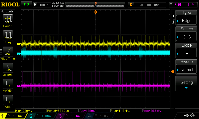
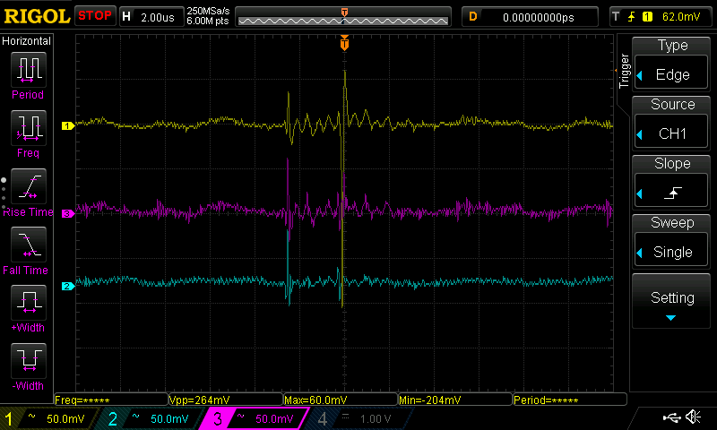
- Lack of power supply decoupling. I didn’t quite realize just how shitty the 24/5VDC power supply is. Sure, I only paid $20 for it, but how bad could it be. The answer is very bad. 240 mVp-p on the 24V rail at full load with proper capacitors on the output. I was getting about half that at lower load, but I didn’t have my instrumentation setup properly for measuring power supply noise (as I learned afterwards from Mr. Dave Jones’ EEVBlog; episode #594), so who knows if the results have any validity. But the noise was most pronounced at ~30KHz, sort of verified using me bumbling around with FFT analysis (again thanks to EEVBlog) , and it fits with general operational characteristics of a switch mode power supply. So I’m running with it. I’ve included some screen shots below from the scope.
- There seems to be a pattern here. After going through the ADC and op-amp docs I have added some rudimentary filtering to all analog inputs. This stuff seemed simpler in my head.
Here are the screen captures from the scope. I did not take very good notes at the time, but I believe channel 1 is the op-amp output, channel 2 is the 5V rail, and channel 3 is the 24V rail.
So there we go. Mistakes have been made. Villages have been burned down. Time to move on.
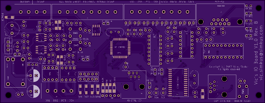
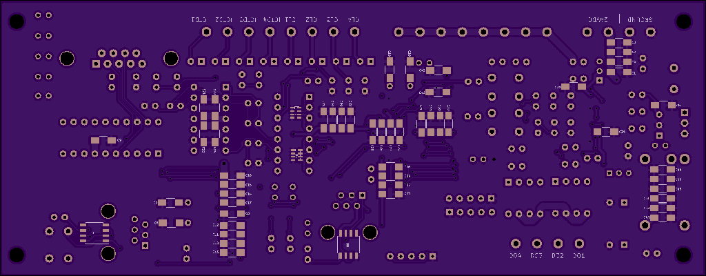
On to REV B
Revision B of the board addresses (hopefully) all (some) of the shortcomings and bone-headed mistakes and maybe adds a little spit and polish.
In no particular order:
- I have incorporated more SMT devices. This board specifically has quite a few 1206 capacitors on it. All LEDs have been changed to 1206 as well. I did not want to. I had to. One of the goals for REV B was to decrease the board size and THT components weren’t cutting it. SMTs have allowed me to use the back side of the board which made a huge difference in space utilization. The optimization was driven by something very real and very near and dear to my heart – the $2/square inch cost of board manufacture at OSH Park that comes out of my beer fund.
- Most of the fuses have been replaced by MIC5013s. Awesome little chip. On the breadboard they were tripping at approximately 107mA with the implementation mirroring the reference design. This is based on the “max” reading of my Fluke 87V. The nice advantage over the fuses is that the trip was “instant” v.s. the slow as molasses trip (relatively speaking) of a fuse. Two of the MIC5013 have been included – one for the analog power output and one for the digital output. Both set to 100mA.
- A Vref+ reference for the ADC has been added. I was checking my ICTD readings against a thermometer not designed by rank amateurs and had quite a bit of a discrepancy. Bit of checking around uncovered that the input to my Vref+ was off by approximately 100mV which threw off the value calculation which was based on the assumption that my ADC range is 0 to 5V.
- Many test points have been added. One of the issues I have on the list is that combining my shitty software stack with my amateurish hardware design is causing a hang of some sorts in my serial communications software. And I’ll be damned if I let all t his test gear sit idle while I fiddle-fuck around for a solution.
- Most of the deficiencies from the previous post have been addressed.
- Oh! The board will only require a single power supply now. I have added a Texas Instruments PTN78000WAH power supply. Super exited to be trying it out.
Below is the renderings of the REV B board as interpreted by OSH Park. The board has been ordered, paid for, and is in fab.
Vic’s Power and Serial Board (VPSB?)
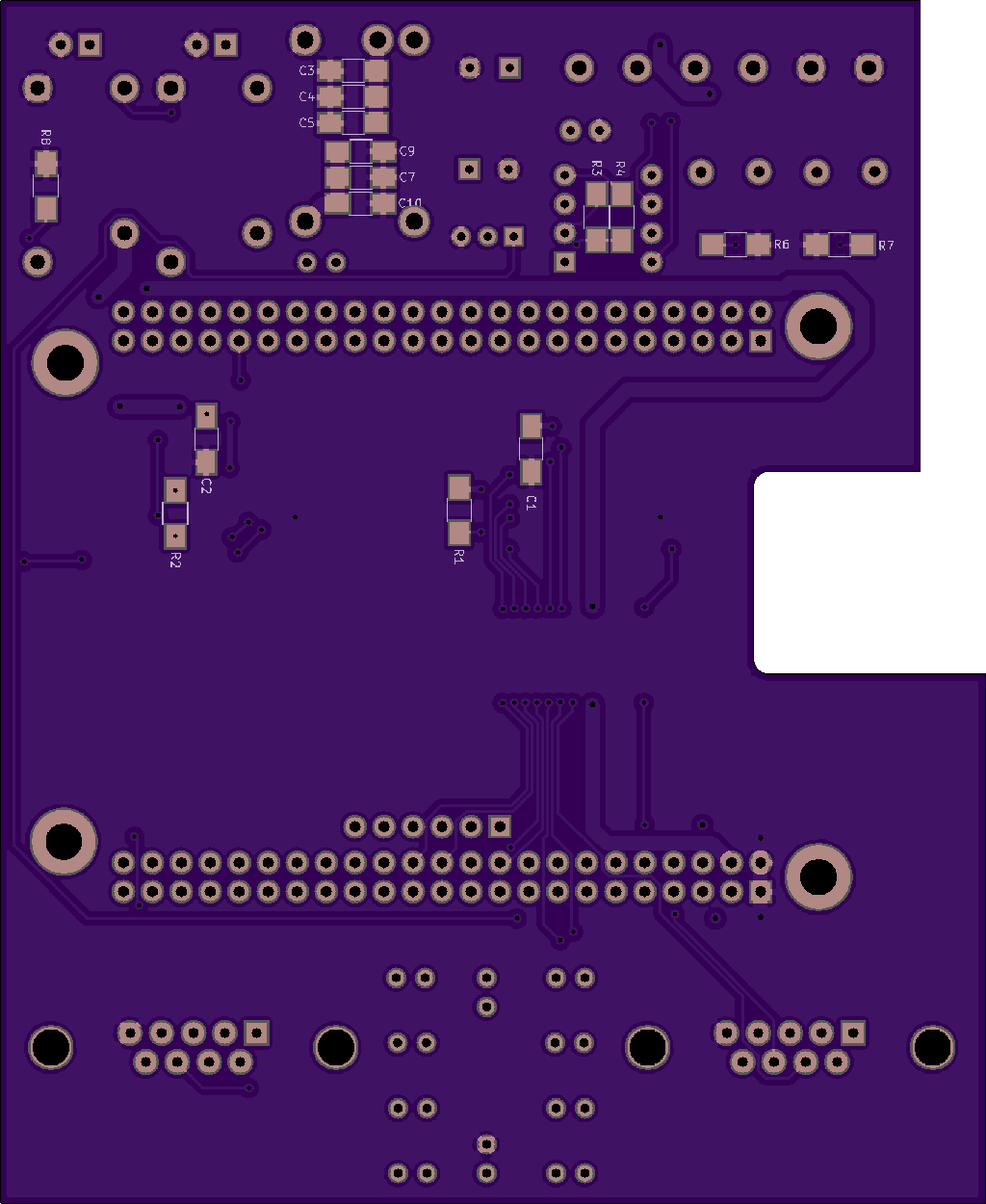
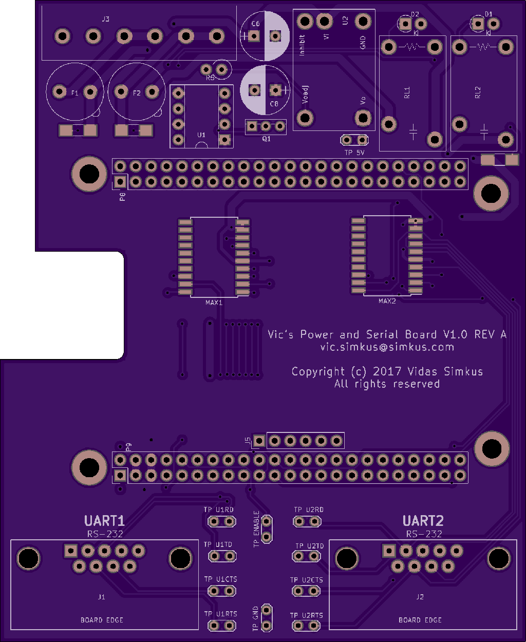
So in order to address the power-up issues of the BBB and in order to break out the serial ports, I had to design my own “cape”. Or is it shield? I can not be bother to Google this set of hipsterisms. It’s an expansion board. Why is it an expansion board rather than a cape or shield or thingamaboob? Well because all those opaque terms is essentially marketing wank. They take a meaning and obscure it using bullshit. If you throw out the term “expansion board” to a general, average or slightly above average intelligence person, they will understand the broad-stroke meaning. They might not know specifically what the fuck you’re babbling about, but they’ll be like: so it’s a board that expands things? And you will be: yes; it’s a board that expands things. And they’ll be like: oh ok. Whatever, geeky computer person. If you throw out the term cape or shield or someotherbullshit term at them they’re gonna think that you think that you’re a super hero and call the hotline.
Ahem.
I had to buy extra parts for this board. The MAX serial driver chips I have on hand are all 5 volt devices. The Beagle Bone is a 3.3 volt device. This is problem.

But it’s done and off to fab.