2017-06-24
2017-06-24
The turkey has landed
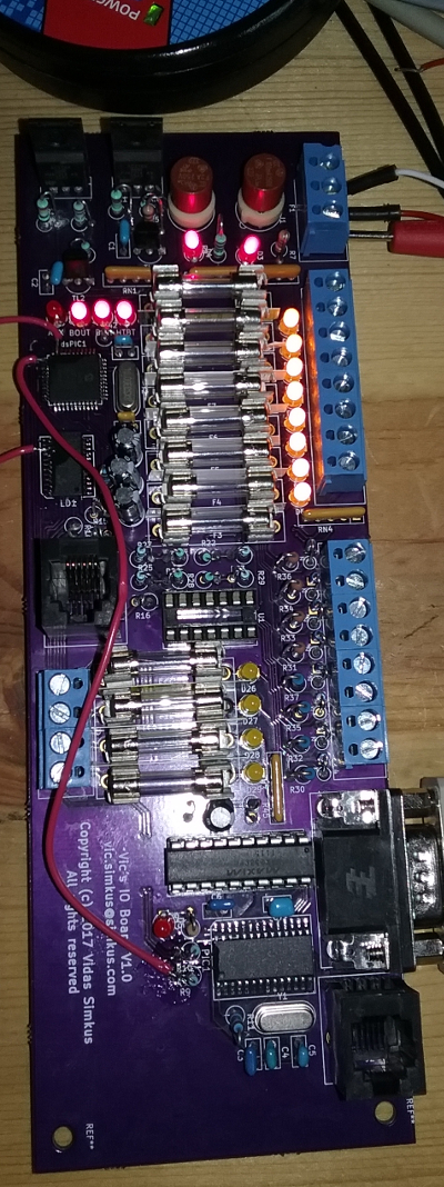
The boards have arrived and the lost Digi-key order has been retrieved. The folks where the package was erroneously delivered were kind enough to reach out to me and I picked it up from them. Assembly wasn’t terrible. Almost everything fit perfectly. I must have double-dosed my stupid pills the day I laid out the pads for the fuse holders. Apparently they’re 9mm wide and I, for some reason, allocated 6mm for them. So they don’t fit. Not even a little bit. I ordered some bare 5x20mm fuse holders and managed to fiddlefuck the fuses in there for testing, but it sucks. In the picture below you can see the pieces of paper I stuck between the fuse holders to keep them isolated.
That was the first just inexcusable bone-headed mistake. The other extra-stupid mistake was a wrong assignment of I2C SDA pin. I was one pin off. Hence the bodge wires in the picture. It was a real treat soldering those on to pins of a surface mount micro. The other bodge wire is to the 24VDC line driver for digital output.
Mo testing mo problems
Besides those two mistakes, below is a list of other mistakes, problems, design considerations, improvements, fixes, and so forth that will be made in revision B of the board.
- I2C pin assignment. Covered above. A case of a plain old oopsie.
- Board reset switch. This is a quality of life issue. It’s kind of a drag to cycle the power supply every time to get the board to cold reset.
- 24VDC LED current limiting resistors are over driven. I failed to take into account the power dissipation of the LED current limiting resistor networks. They’re essentially heaters now. In rev B the resistor will be changed from 1.5K to 4.7K.
- Standardize the 5VDC LED current limiting resistors. Right now it’s a mix of 220 and 470 ohm resistors. In rev B they will all be 470 ohm.
- Fix IO controller (dsPIC33) status LED terminations. Right now the anode/cathode are swapped around in the schematic requiring them to be installed in the board opposite of the silk screen graphic.
- Space allocated for fuse holders is too small 6mm are allocated, but 9mm are needed.
- Resistor “orientation” is inconsistent. Yes I know resistors are not directional, but since I am installing them vertically some of the silk screen graphics are mirrored in order to make the trace layout easier. This is purely an aesthetic issue.
- Will be adding power supply decoupling capacitors.
- Convert overcurrent protection from fuses to a PMIC setup. More on that below.
- Current limiting resistors for analog input overvoltage protection clamp diodes. Blew some up in testing. Lessons have been learned.
- Implement chip sanity monitoring for both microcontrollers.
- Change to single input voltage. More on that below.
- Remove trace width transition “resistors”. I had put in several resistor pads that used a jumper in order to facilitate trace width change. I did that because I didn’t know how to do that in KiCad. I do now and they will be removed in rev B. On the other hand they were really handy for testing and scope probe attachments.
- Component references are a mess. I deliberately did not pay attention to those in the initial design, but assembly would have been so much easier if the references were better organized.
Deliberate dead short
In my travels through the industrial refrigeration world the one thing that never ceases to amaze me is the myriad of ways that electric and electronic components and systems fail. The systems are designed to take lots of abuse and neglects, but when they fail oh boy is it a show. In the design of my board I wanted to minimize the impact of external failures.
On the power input I put in two crowbar circuits – one for the 5VDC input and one for the 24VDC input. The reasoning was that if the power supply went haywire the crowbar circuit would activate and blow the fuse rather than allowing on over-voltage condition propagate and damage the board components.
On the analog input I put in Schottky diodes to clamp the incoming voltage to bellow 5.5VDC which is the limit for the ADC input of the dsPIC33. The reasoning was:
- Analog input voltage rises above 5.4 (0.4 being the Vf of the the diode).
- The diode becomes forward biased and dumps into the 5VDC rail.
- The 100mA fuse on the +24VDC supply to that analog input blows eliminating the power supply to that analog input.
- In case the power supply can not bring the voltage down on the 5VDC rail the crowbar circuit activates and acts as a final safety
- Damage to the microcontroller ADC input is prevented.
So elegant in my head. I tested the operation by connecting a wire from the 24VDC output of the analog input directly to the input. Here’s what actually happened.
- 24VDC from the analog output is connected directly to the input.
- The diode becomes forward biased and dumps into the 5VDC rail.
- The 100mA fuse on the 24VDC supply to the analog input does not blow.
- The power supply does not ramp down gracefully.
- The crowbar circuit activates.
- The crowbar circuit does not blow.
- The power supply freaks out and shuts down on dead short protection.
- The crowbar circuit releases.
- The power supply comes back to life.
- Repeat from step 2 a few times until the crowbar fuse FINALLY blows.
Very not elegant. During testing one of the clamping diodes gave up the ghost. Like super not elegant!
Spent some time diving deeper into fuse design and they’re not as simple as I thought. Like super not as simple as I thought. I was under the impression that a 1 amp fuse, for example, just blows when more than 1 amp is applied across it. But there are a myriad of variables that influence the trip currents and the timing of the trip. Too complicated. Complication equals fragility and I don’t like fragility. Not to mention all those fuses take up a ton of board space and the fast-blow low-amperage fuses cost an arm and a leg. Need a better design.
To the rescue comes PMIC – power management integrated circuits. I didn’t know about this little gem during rev A design. I will be using two Microchip MIC5013. One will be used for analog input power outputs and one will be used for the digital outputs. Both will be configured for a trip point of 100mA. A nice side benefit of using a PMIC is that all of the 4x20mm fuses will be not be needed thus freeing up a lot of space on the board.
Another major change in the power supply is going to a single 24VDC input and stepping it down to 5VDC using a Texas Instruments PTN78000W. This will simplify installation, circuit design, and free up space on the board since I will no longer need a 5VDC crowbar circuit. I will retain the 24VDC crowbar and input fuse.
On the next episode
Testing testing and more testing. I want to hit every corner case I can think of before finalizing the rev B design. The next victims are reading analog input values via the microcontroller and doing digital output.