2017-06-08
2017-06-08
The design of the power and serial cape is done. The components have been ordered. I will wait until the IO board comes back and the components come in before sending the cape off to fab. Juuuuust to make sure I didn’t screw up some minute detail that renders the design useless.
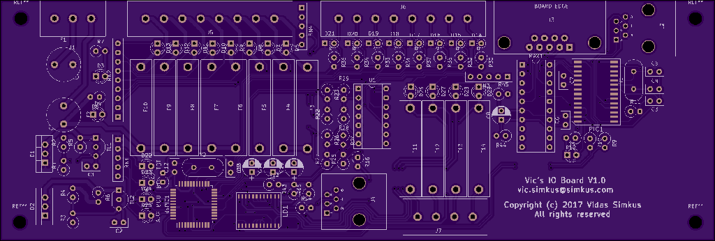
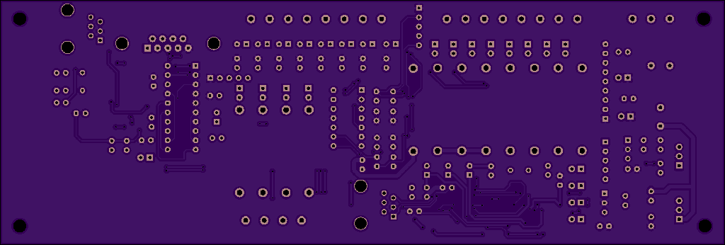
Additionally, I found a high-resolution picture of the IO board PCB in ‘as made’ representation on the OSH Park’s website. Neato.
Front:
Back:
And here’s the cape as it will be if everything checks out:
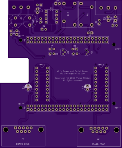
The cape could be made more compact. While the power section fits like a glove, the section holding the DB9 connectors can be compacted quite a bit. The upside is that the cost would be reduced because the total board area would be reduced. The downside is that the cape would then be asymmetrical. I’ll probably go with the more expensive, but more aesthetically pleasing option.