2017-09-09
2017-09-09
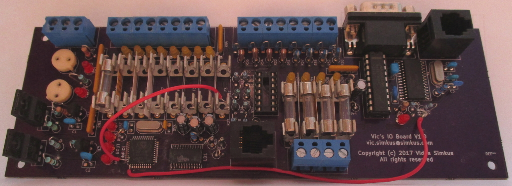
It appears that I am incapable of taking a decent picture. I guess I am not perfect after all. All of the pictures below were taken at the same time. Well OK technically not at the same time; they were taken in a serial fashion. They were taken during the same picture taking session. Why some of them look like a teenage girl applied some sort of social media photo filter on them is beyond me.
Anyways.
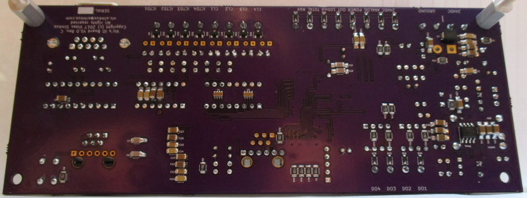
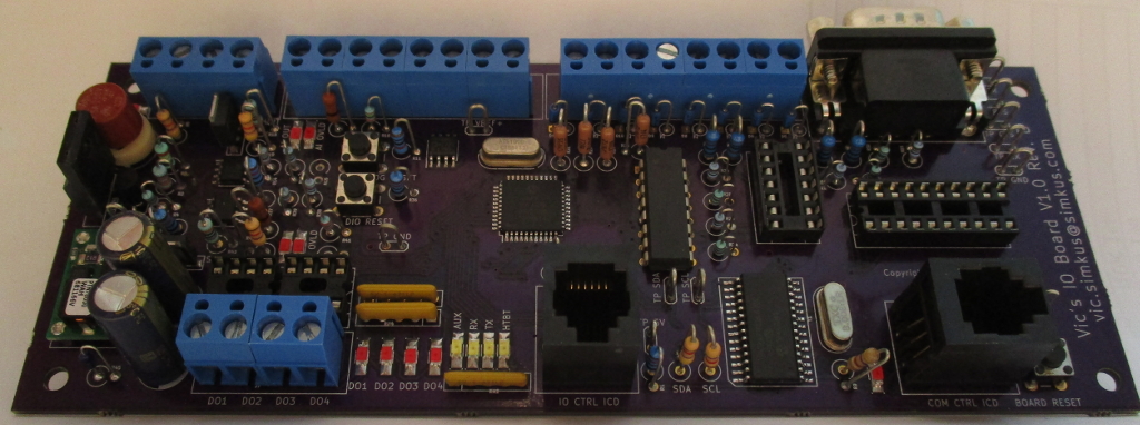
I’m actually pretty excited how revision C came out. Initial testing shows that everything is functional. We have full comms – I2C and RS-232, analog inputs are fairly stable, over-current protections are fully operational, and reverse polarity protection on-point.
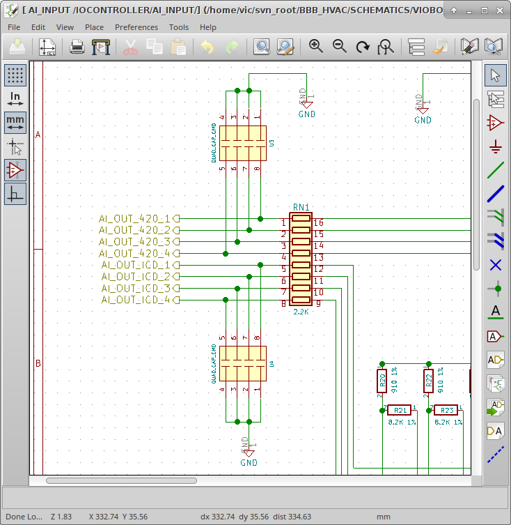
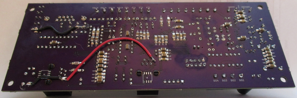
The greatest success story is the analog front-end, if I may borrow terminology to make my minuscule achievement sound more impressive than it actually is. In revision B I added a low-pass filter upstream of the ADC and it has done wonders. The firmware (the ADC portion anyways) has remained the same as in rev A, but the readings are rock steady. In rev A the ADC output was all over the place. In rev C (same configuration as rev B) the values coming out of the ADC are simply beautiful. I attribute it all to the low-pass filter I put in the design. Thank you, Microchip application note.
The RC low-pass filter.
Below is a photographic timeline of the revisions. Looking back, revision A looks down right crass. A plethora of things have been learned during the process of getting to revision C and I am anxious to put them to use in future projects.
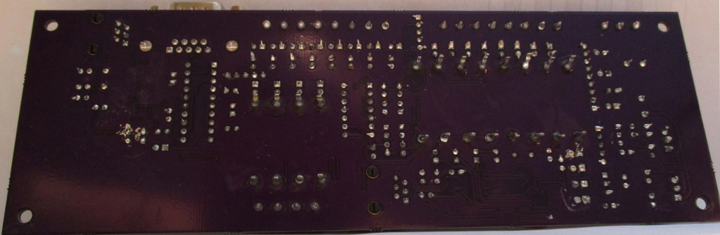
Version 1.0 – Revision C
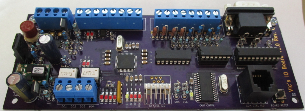
Version 1.0 – Revision B
Version 1.0 – Revision A